


|
Nanostructured thin films
D. Nesheva, Z. Levi, Z. Aneva, I. Bineva
The work in the field was initiated by Prof. Elena Vateva more than 20 years ago with fabrication and characterization of amorphous multilayers based on selenium. Recently, the attention has been concentrated on formation and investigation of crystalline and amorphous semiconductor nanoparticles and nanocrystalline single layers.
Thermal evaporation in vacuum is used to produce II-VI (CdSe, ZnSe, CdS) thin and ultra thin single layers. Two deposition approaches are applied: one-step deposition during which the substrates are fixed above the crucible and step-by-step deposition which involves the rotation of the substrates at a rate varying between 8 and 30 cycles/min as the substrates spend only 1/12 part of the cycle over the source. This approach allows fabrication of multilayers with smooth interfaces and well defined layer thickness.
|
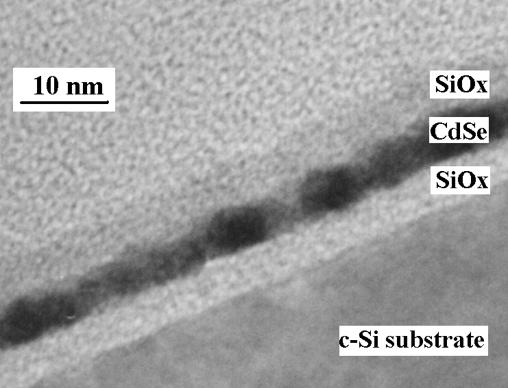
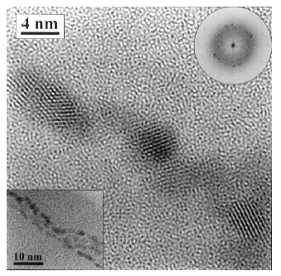
2. Self-asembling of CdSe nanocrystalsNanocrystals of CdSe embedded in amorphous SiOx, GeS2 and polycrystalline ZnSe thin film matrix (composite films) are successfully produced using a multilayer approach. Step-by-step physical vapor deposition of CdSe ultra thin films on the relative ‘rough’ surface of ‘one-step’ deposited layers from the matrix materials is applied. The matrix layer thickness is 20 times greater than the CdSe one. High-resolution electron microscopy proved the formation of CdSe nanocrystals with nearly spherical shape. The particles are partly isolated and partly in contact and their spatial distribution follows the surface morphology of the ‘matrix’ films. The average size of the nanoparticles is about two times greater than the nominal thickness of CdSe layer. The annealing of SiOx- CdSe films at proper high temperatures allows formation of isolated CdSe nanocrystals homogeneously distributed in the SiOx matrix.
|
3. Growth of Si nanoparticles in SiOx matrixSiOx thin films with various oxygen contents (1.1?x?1.7) are produced by thermal evaporation of SiO in vacuum. The film composition is varied by varying the deposition rate and residual pressure under the vacuum chamber. Amorphous and crystalline Si nanoparticles are grown by furnace and rapid thermal annealing at various temperatures, for various times and in various ambients. Visible photoluminescence is observed at room temperature which, in the films with the same initial composition, is stronger in the films containing amorphous Si nanoparticles than in those having nanocrystals.
Ěetal-oxyde-silicon (MOS) structures containing layers with amorphous or crystalline silicon nanoparticles in a silicon oxide matrix are fabricated by sequential physical vapour deposition of SiOx and RF sputtering of SiO2 on p- or n-type crystalline silicon, followed by high temperature annealing in an inert gas ambient. Depending on the annealing temperature, 700oC or 1000oC, amorphous or crystalline silicon nanoparticles are formed in the SiOx. High frequency C-V measurements demonstrate that these structures are suitable for production of nonvolatile memories. |

Sample characterizationX-ray diffraction, high resolution electron microscopy and Raman scattering measurements are carried out (in collaboration with several European Institutes and Universities) in order to study the shape, structure, spatial and size distribution of CdSe and Si nanoparticles as well as to investigate material intermixing in both multilayers and composite films. |
Collaboration• Institute of Physics, Carl von Ossietzky University Oldenburg, Oldenburg, Germany; • Dundee University, Dundee, Scotland, UK; • Institute of Physics, Center for Solid State Physics and New Materials, Belgrade, Serbia; • National Polytechnical University of Athens, Greece;
• Max-Plank Institute of Microstructure Physics, Halle, Germany. Recent publications |
Last update February 2007
Copyright © 2007